
Encapsulating Electronics Without Potting or High-Cost Tooling
Protecting electronic assemblies from moisture, vibration, and mechanical damage has traditionally meant one thing: place the electronics into a housing and flood the assembly with a two-part potting compound.
While effective, this approach often brings unnecessary cost, long cycle times, and significant design constraints.
As product lifecycles shorten and development budgets tighten, manufacturers are increasingly questioning whether potting is always the right answer.
At Nordell, we believe there is a practical and proven alternative.
Rethinking Electronics Protection
Potting is widely understood and trusted, but it is not without drawbacks.
Two-part materials have limited working lives, cure times slow production, and separate housings introduce additional tooling, components, and assembly steps.
In many cases, the requirement is simple: protect the electronics and deliver a robust finished part. The challenge is achieving this without adding unnecessary complexity.
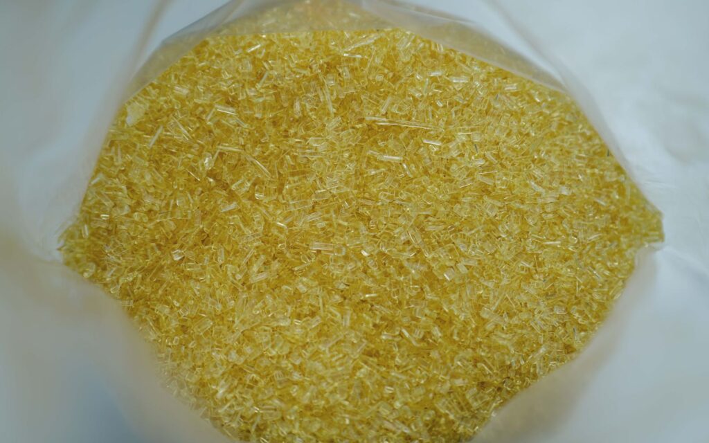
Low-pressure injection moulding offers a different way to encapsulate sensitive electronics.
Using Technomelt PA673N amber, a low melt, low pressure nylon-based material, electronic assemblies can be placed directly into a mould cavity and overmoulded.
The polymer flows gently around components, fully encapsulating them without causing thermal or mechanical damage.
Rather than moulding a housing and then potting, the encapsulation and the external geometry of the finished part are formed in a single process using plastic injection moulding services.
This removes the need for separate housings, two-part potting compounds, long cure times, and secondary operations.
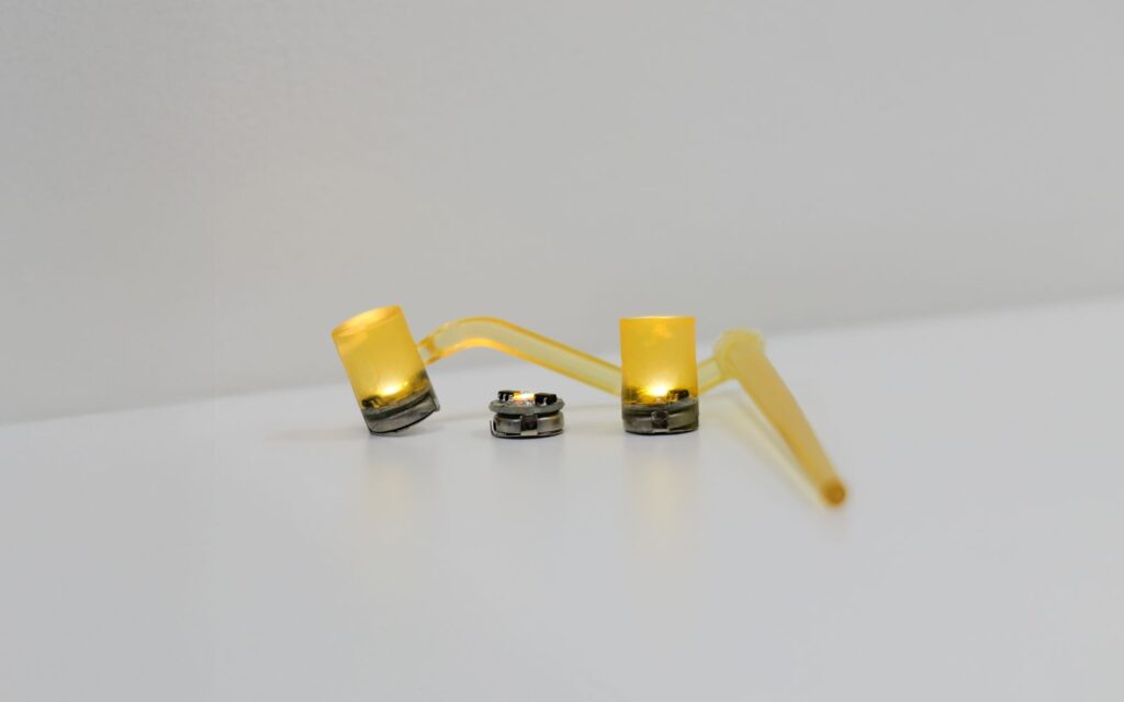
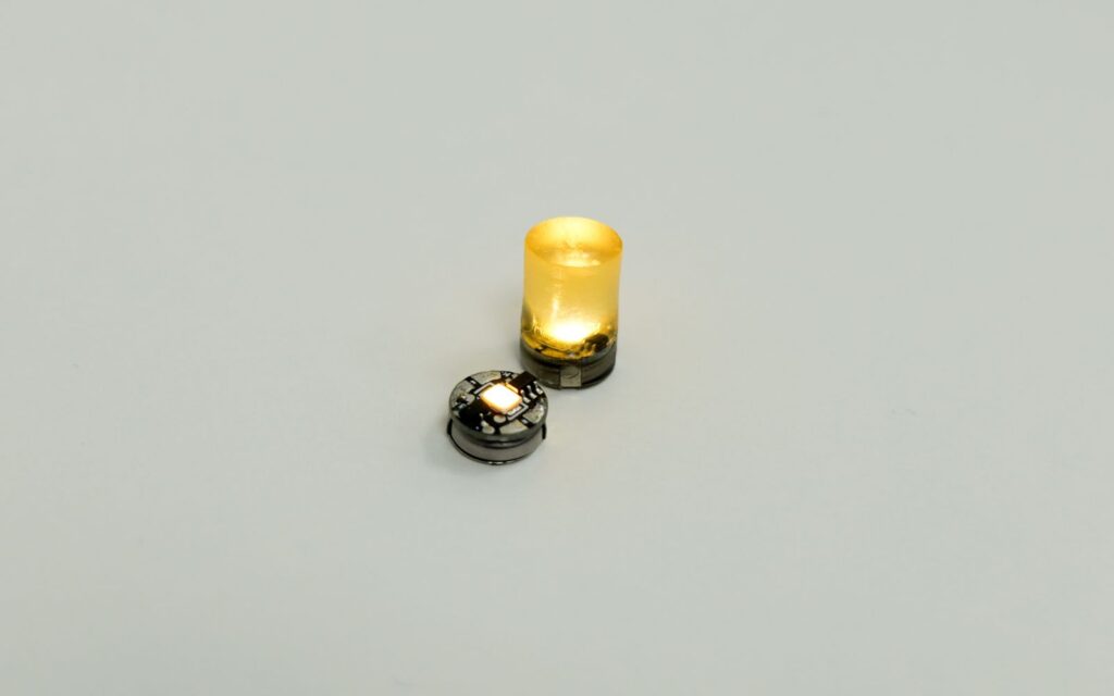
To validate this approach, Nordell has completed proof-of-concept trials using small electronic circuit boards fitted with LEDs.
The boards were overmoulded directly using Technomelt PA673N amber, fully encapsulating the electronics. After moulding, the LEDs remained fully operational.
This is a critical point. These were live electronic assemblies, not dummy components. The trials demonstrate that sensitive electronics can be safely encapsulated using this process without compromising functionality.
Why Rapid Tooling Changes The Equation
One of the biggest barriers to overmoulded electronics has traditionally been tooling cost.
This is where rapid tooling and additive manufacturing play a key role.
Nordell has demonstrated that Technomelt PA673N amber can be successfully moulded into 3D-printed injection mould tools made from rigid, ceramic-like materials such as Formlabs 10K resin.
This approach enables:
- Low-cost tooling for proof of concept and early production
- Rapid turnaround from design to moulded part
- Straightforward iteration of cavity geometry
- A low-risk entry point for feasibility studies
In many cases, this removes the need to invest in high-cost steel tooling until designs are fully validated or volumes justify it, reducing risk before committing to full tool manufacture.
Design freedom and functional integration
Overmoulded encapsulation also unlocks greater design freedom than traditional potting.
Because the polymer defines both protection and form, it becomes possible to integrate features directly into the moulded part, including:
- Strain reliefs for cabled electronics
- Sealed cable exits and connectors
- Overmoulding around displays, buttons and control interfaces
- Application-specific external geometries
The result is a cleaner, more integrated design with fewer components and assembly steps.
Where This Approach Delivers The Most Value
This combined process is particularly well-suited to:
- Encapsulated electronic modules
- Sensors and control units
- LED assemblies
- Cabled electronics requiring integrated strain relief
- Low to medium volume products and development programmes
It delivers cost savings by removing potting materials and processes, time savings through shorter cycle times, and commercial flexibility through low-cost tooling — while also simplifying downstream assembly and finishing.
A Proven, Underused Solution
Low-pressure overmoulding of electronics is not a new idea, but it is one that is often misunderstood and underused.
By combining the right material with the right tooling approach, it becomes a practical, low-risk manufacturing route that challenges the assumption that potting is the only option.
If you are attending Southern Manufacturing, come and talk to the team.
We have real moulded parts, printed tooling, and working proof-of-concept demonstrations to show what is possible.
Alternatively, get in touch to discuss whether this approach could work for your application.